Okay, let’s be real for a minute here. Usually, when the European Union announces some grand new tech initiative, the collective reaction from the global tech community is a polite nod—maybe a stifled yawn—before everyone goes back to doom-scrolling through the latest hype coming out of Silicon Valley or Shenzhen. We’ve become conditioned to view Europe in a very specific, somewhat unexciting light: they’re the regulators, the referees, the “ethical compass” of the industry. But the engine of raw, bleeding-edge hardware innovation? Not so much.
That narrative, however, might finally be starting to shift. or at the very least, it’s getting a massive, €700 million shove in a different direction.
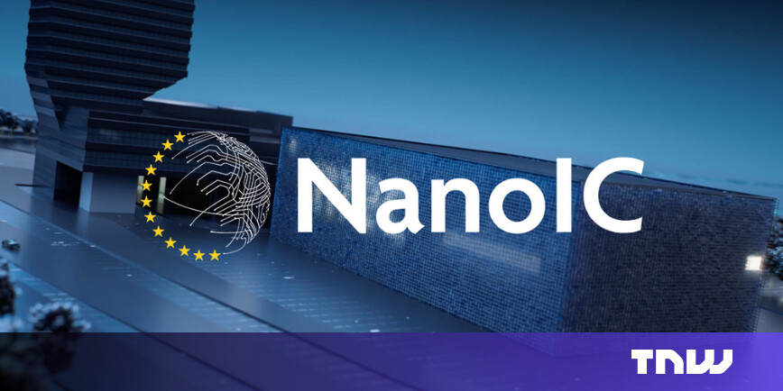
As reported by The Next Web, the EU has officially cut the ribbon on NanoIC, a brand-new semiconductor pilot line nestled within the hallowed halls of Imec in Leuven, Belgium. If you aren’t familiar with Imec, think of it as the Hogwarts of nano-electronics. It’s the place where the actual magic happens—where the physics gets bent and the future gets built—long before the rest of the world figures out how to bottle it and sell it. This isn’t just another bureaucratic photo-op with oversized scissors; it’s a tangible, silicon-and-steel manifestation of the European Chips Act coming to life.
But here is my hot take on this: while the headline number is obviously the cash, the real story here isn’t the money. It’s the model. We are looking at a fundamental shift from “Europe makes rules” to “Europe makes prototypes.” And in the brutal, capital-intensive world of sub-2-nanometer chips, that distinction is absolutely everything.
Surviving the Hardware “Valley of Death”
There is a notorious concept in the deep tech world known as the “Valley of Death.” It sounds dramatic, but it’s an accurate description of that treacherous, resource-sucking gap between achieving a brilliant breakthrough in a university lab and actually getting a commercially viable product rolling off an assembly line. In the software world, crossing this gap might cost you a few laptops, some server space, and a heck of a lot of coffee. But for semiconductors? You’re talking about burning through billions before you see a dime.
This is exactly where NanoIC is stepping in to bridge the divide. The facility is designed as an “open pilot line.” Now, I know that sounds like dry corporate jargon, but it’s actually a pretty radical democratization of access. Under normal circumstances, if you want to play around with 2-nanometer transistors—the kind of bleeding-edge tech that powers the absolute fastest AI models and next-gen weaponry—you generally need to be Apple, NVIDIA, or have a direct line to the CEO of TSMC. The velvet rope is incredibly exclusive.
NanoIC effectively changes the access codes. It throws open the doors to startups, smaller enterprises (SMEs), and research institutes that would usually get laughed out of the room if they asked for fab time at a major commercial foundry. Suddenly, these smaller players can prototype System-on-Chip (SoC) technologies that, technically speaking, don’t even exist in the commercial market yet.
“By lowering barriers to access for SMEs and research organisations, the initiative seeks to diversify Europe’s semiconductor ecosystem and catalyse new product development without the massive upfront costs of commercial fabs.”
— The Next Web
Why does this matter? Because right now, innovation is getting strangled by cost. When a single cutting-edge lithography machine costs as much as a jumbo jet, the number of players who can afford to innovate shrinks drastically. Europe is essentially stepping in to subsidize the entry fee for the little guys, betting on the hope that the next NVIDIA isn’t born in a garage in Santa Clara, but in a lab in Leuven.
Beyond the Specs: Why Sub-2-Nanometer Tech Actually Matters
Let’s geek out for a moment on the actual specs, because this is where it gets interesting. The pilot line is hyper-focused on “beyond-2-nanometre” technologies. In the semiconductor world, the rule is simple: smaller is better, faster, and more power-efficient. But we are currently slamming headfirst into the laws of physics. Shrinking transistors any further isn’t just about making things smaller; it requires exotic materials and entirely new architectures like Gate-All-Around (GAA) or Forksheet transistors (which happens to be an Imec specialty).
Getting this right is crucial for the ongoing AI boom. We are currently insatiable when it comes to compute power. Training the massive large language models of 2026 and beyond is going to require a level of energy efficiency that our current chips simply struggle to provide. If Europe can corner the market on the design and prototyping of the most efficient AI chips, it gains a leverage point that no amount of GDPR legislation can ever provide.
And it’s not just about AI, either. We’re talking about the backbone of 6G communications, autonomous systems that need to process terabytes of data in milliseconds without melting your car’s dashboard, and health tech microscopic enough to live inside the human body. These aren’t just “faster phones”; they are the invisible infrastructure of the next decade.
The Sovereignty Play: Why Europe is Anxious About Supply Chains
We really can’t talk about chips these days without talking about sovereignty. It’s the buzzword of the decade for a reason. If the pandemic taught us anything, it’s that relying on a single, fragile supply chain for critical components is a fantastic way to cripple your entire economy overnight. The EU has been sweating over its heavy reliance on Asian manufacturing and American intellectual property, and they are tired of feeling vulnerable.
The Chips Act, which is backing this €700 million investment (as part of a much larger €2.5 billion program), is effectively Europe’s attempt to buy some insurance. According to the European Commission’s original targets, the goal is to double Europe’s global market share in semiconductors to 20% by 2030. Are we on track for that? That’s highly debatable. But initiatives like NanoIC are the concrete, steel-in-the-ground steps needed to even have a shot at getting there.
It’s also worth noting exactly who is sitting at the table here. ASML is involved. This is critical. ASML is the Dutch company that builds the machines that build the chips. They are arguably the most important tech company in the world that nobody outside the industry talks about enough. Having them directly integrated into this pilot line means the feedback loop between the toolmakers and the chip designers is going to be incredibly tight, accelerating the whole process.
Is €700 Million Actually Enough to Move the Needle?
Now, here is the counterargument, and honestly, it’s a strong one. €700 million is a staggering amount of money to you and me. But in the semiconductor industry? It’s a rounding error.
To put that number in perspective, building a single modern commercial fab—like the massive plants TSMC is constructing in Arizona or Intel is planning for Magdeburg—costs upwards of €20 billion. A recent report from Reuters highlighted that the total investment required just to keep pace with Moore’s Law globally is in the hundreds of billions annually. It is a game of astronomical stakes.
So, is €700 million going to turn Europe into a manufacturing superpower overnight? No. Absolutely not. If you think this money means we’ll see “Made in Belgium” stamped on the processor of your next iPhone, you’re mistaken.
But thinking that way is missing the point. NanoIC isn’t about mass manufacturing. It’s about IP creation. It’s about owning the blueprints. The U.S. designs the chips, Taiwan manufactures them, and the Netherlands (ASML) builds the machines. Europe wants to drastically expand its role in that “design and research” phase. If the next breakthrough in chip architecture comes from a startup incubating in NanoIC, the manufacturing can happen anywhere, but the royalties, the patents, and the strategic control stay right here.
Breaking Down Silos in a Secretive Industry
One of the most promising aspects of NanoIC is its collaborative nature. The facility is bringing together officials from the European Commission, industry heavyweights, and academic leaders. It’s a “Chips for Europe” initiative in the truest sense of the phrase.
We are seeing a necessary move away from the siloed, secretive nature of chip development. Traditionally, companies guard their processes like state secrets. And, to be fair, they still will. But the pre-competitive research—the deep science stuff that happens before a product is even defined—benefits massively from shared brainpower. By creating a neutral ground at Imec, the EU is fostering an ecosystem where cross-pollination can actually happen.
This is vital for the talent pipeline as well. You can’t have a thriving semiconductor industry without engineers who know how to work with extreme ultraviolet lithography (EUV). NanoIC serves as a high-end training ground for the next generation of talent, addressing a skills gap that is just as threatening to the industry as the supply chain issues.
So, What’s the Verdict?
It’s easy to be cynical about EU tech initiatives. History is littered with the corpses of “European Googles” that never happened. But semiconductors are different. Europe already has a legitimate stronghold here thanks to Imec and ASML. We aren’t trying to catch up from zero; we are trying to leverage an existing superpower.
NanoIC represents a smart, targeted bet. It’s not trying to out-spend the U.S. or out-manufacture China. It’s doubling down on what Europe does best: complex, high-level research and engineering. By bridging the gap between the lab and the fab, the EU isn’t just throwing money at a problem—it’s building a bridge.
The success of this pilot line won’t be measured in the next six months. It will be measured five years from now, when we look at the spec sheet of a revolutionary new AI accelerator or a 6G modem and see that its journey began in Leuven.
This article is sourced from various news outlets. Analysis and presentation represent our editorial perspective.